


As energy saving becomes a major social issue, adoption of inverters for distributed power generation, such as photovoltaic, wind, or fuel cell devices, new renewable energy, and energy saving has garnered tremendous interest. This power semiconductor module is a core component of Power Conditioning Units (PCU), industrial inverters, Uninterruptible Power Supplies (UPS), and large-capacity Power This paper investigates a high-efficiency high-voltage Trench Gate Field Stop IGBT, a core component of industrial inverters to raise the energy consumption efficiency of power conditioning unit and motor for distributed power generation photovoltaic, wind, and fuel cell devices.
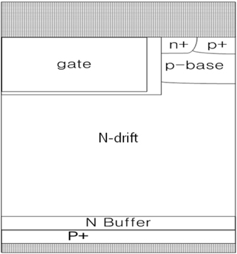
2.1 Basic design of a 1,200 V Planar type NPT IGBT
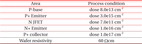
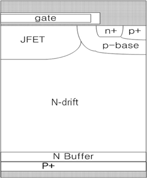
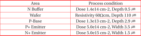
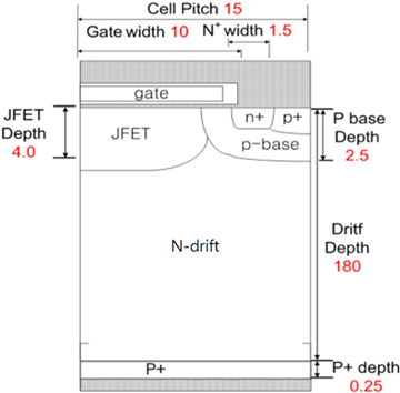
The primary matters to consider in designing a 1,200 V Planar type NPT IGBT are (1) the resistivity of wafer and (2) the drift layer thickness of the device to design. For this, an IGBT with a structure as in Fig. 1 was designed with the process conditions found in Table 1.
[Table 1.] Basic process parameters.

Basic process parameters.
2.2 Breakdown voltage simulation according to drift thickness
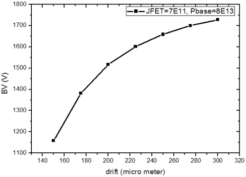
As the drift layer thickness increases, the breakdown voltage increases, but at over 200 ㎛ the increase width reduces dramatically. Here, the maximum length of a depletion layer is 157 ㎛, so smaller lengths a punch-through phenomenon occurs. Besides, as the drift thickness increases, the on-state resistance increases, and can be viewed as a reasonable trade-off.
In order to avoid the punch-through phenomenon and achieve the target breakdown voltage, the ideal drift thickness was determined as 180 ㎛ and the wafer resistivity was determined as 60 Ωcm. At these conditions the target breakdown voltage and low on-state voltage drop, which is suitable for the design of a 1,200 V Planar NPT IGBT. In addition, the structure holds only when the Field-Stop IGBT design has a less than 157 ㎛ drift thickness.
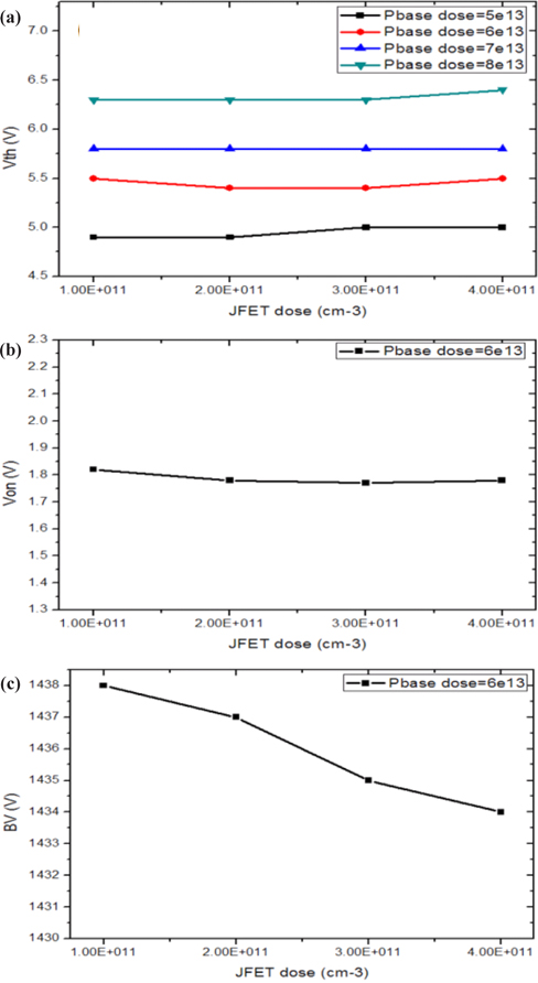
2.3 The electrical characteristics according to dose of P-base and JFET region
A simulation was carried out while adjusting the N JFET and P base dose to 1e11 ~ 4e11 cm−2 and 5e13 ~ 8e13 cm−2, respectively, in order to optimize the Planar type NPT IGBT after setting the wafer resistivity and drift layer thickness. With the threshold voltage aimed at about 5.5V, for which the threshold voltage varied according to the JFET and the P-base dose, which was determined as 6e13 cm−2.
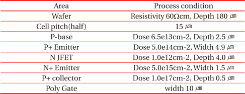
[Table 2.] Planar NPT IGBT Final process parameters.

Planar NPT IGBT Final process parameters.
As the JFET dose increases, the resistance in the JFET area decreases, so the on-state voltage drop is expected to reduce, but was found to have a little to no effect. This is due to the JFET resistance is very low since the concentration in the JFET area is high enough. The optimized process variables were set through a simulation on the variables related to the P-base dose, and was confirmed that the threshold voltage was 5.5 V, the on-state voltage drop was 2.35 V (for 100 A), and the breakdown voltage was 1,425 V.
[Table 3.] Planar NPT IGBT Final process parameters.

Planar NPT IGBT Final process parameters.
2.4 Basic design of a 1,200 V planar Field Stop IGBT
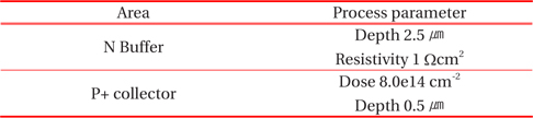
Based on the 1,200 V Planar type NPT IGBT design technology, the design of a Planar type FS IGBT was executed. The generation of punch-through was hindered by induces the punch-through to occur and induce a sudden drop of electric fields through insertion of N buffer layers via reducing the drift layer thickness of an optimized Planar type NPT IGBT. The inserted N buffer layer was assumed to have a uniform concentration in the simulation, rather than a wafer back process with the thickness was found to be 2.5 ㎛.
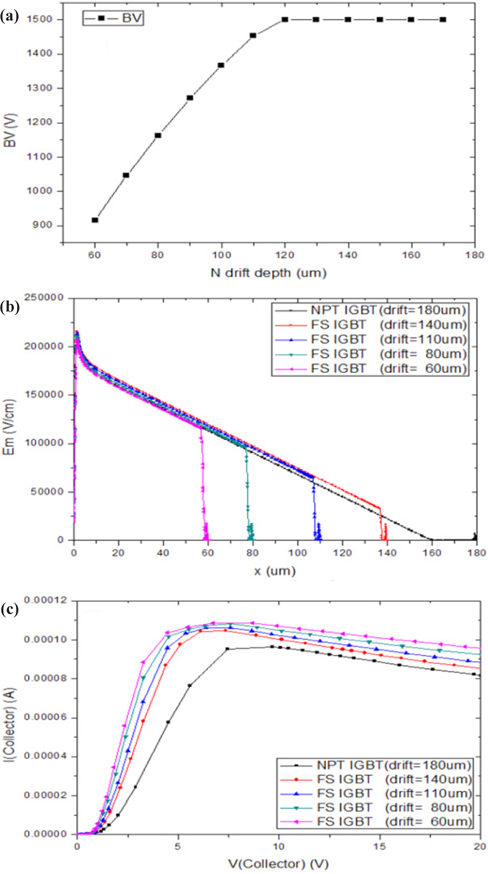
2.5 The electrical characteristics of planar NPT FS IGBT according to N drift thickness
The thickness of the spare drift layer of the previously designed NPT IGBT was 22 ㎛, thus the thickness of the drift layer was determined to be 157 ㎛ or less to observe an increase in breakdown voltage pursuant to the insertion of N buffers. A trade-off relationship was confirmed so that the breakdown voltage and on-state voltage drop reduce together as the thickness of the N drift layer decreases in concentration and length of the preferably assumed N buffer, and the drift thickness was determined as 110 ㎛ to achieve the target.
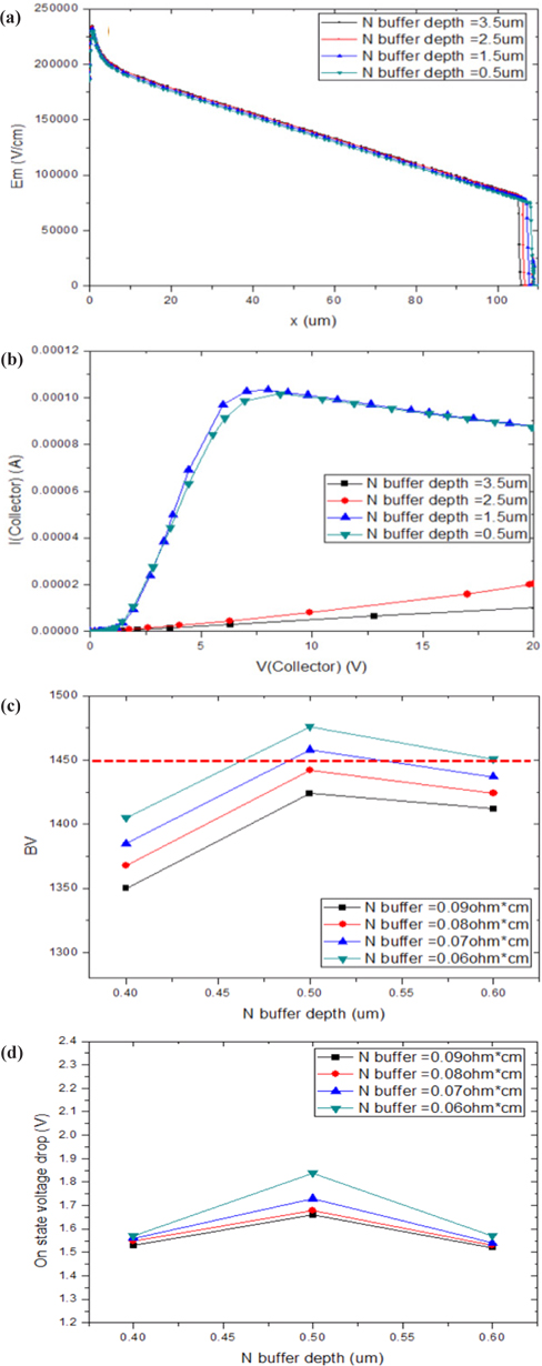
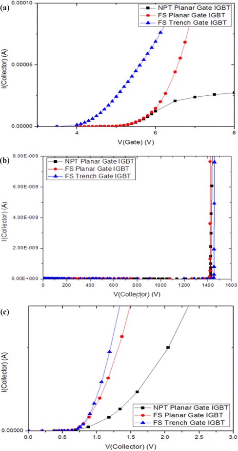
The result value of the previous experiment was fixed, and then the thickness of the N buffer was adjusted. As shown in Fig. (a) and (b), the thickness of the buffer layer does not affect the breakdown voltage but as the thickness of the buffer layer decreases, the on-state voltage drop reduces. As shown in Fig. 5 (c) and (d), the thickness of the buffer layer meets the target breakdown voltage at 0.5, but the on-state voltage drop has a slightly higher value of 1.9 V
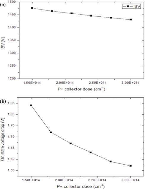
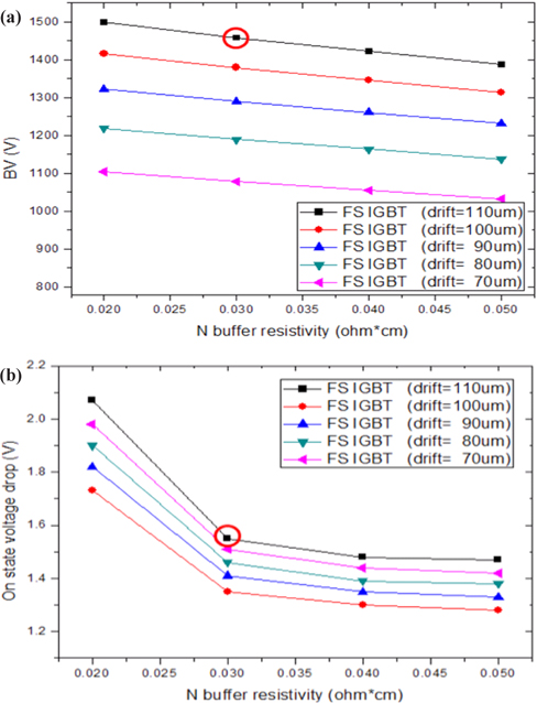
After changing the thickness and concentration, the hole insertion efficiency at the P+ collector significantly reduced, the conductivity modulation effect was also reduce, and the on-state voltage drop significantly increased. Accordingly, as a result of changing the P+ collector concentration in a structure of buffer concentration 0.06 Ωcm and buffer thickness 0.5 ㎛, the on-state voltage drop reduces due to high hole insertion efficiency. However, due to an increase in P+ collector concentration, the thickness of the N buffer layer, the internal charge capacity, the maximum point of the electric field applied to the N buffer layer, and the breakdown voltage reduces. At this time, as shown in Fig. 9, the trade-off optimum point between the breakdown voltage and the on-state voltage drop could be obtained as a result of adjusting the P+ collector concentration, and the concentration and thickness of the low N buffer was applied to obtain optimized properties: the drift thickness of 110 ㎛, buffer resistivity of 0.03 Ωcm, buffer thickness of 0.5 ㎛, breakdown voltage of 1,458 V at P+ collector dose 1e15 cm−2 and on-state voltage drop of 1.55 V.
[Table 4.] Planar NPT IGBT Final process parameters.

Planar NPT IGBT Final process parameters.
2.7 Design of 1,200 V Trench Gate NPT Field Stop IGBT
Based on the 1,200 V Planar type FS IGBT design technology, a Trench type FS IGBT was designed and the electrical properties of the NPT IGBT and Planar type FS IGBT were compared.
At this time, the threshold voltage was set to 5.5 V, and the P-base dose for this was fixed at 8.0e13 cm−2. The buffer simulation condition of the Trench type FS IGBT is the same as the condition of the Planar type IGBT. However, the simulation depending on width and length of the trench gate executed and summarized in Table 1. At this time, the on-state voltage drop reduces as the gate depth deepens while the trench gate width remains unchanged. The electric field concentration phenomenon at the bottom of the trench gate strengthens as the gate depth deepens.
An optimized structure has been designed for each device, and the comparison results of the electrical properties of each IGBT are shown in Table 8 below. As shown in Table 8, the threshold voltage dropped, the breakdown voltage was high and the Vcesat reduced as compared to the Planar and Trench.
In this paper, we have analyzed the electrical characteristics of 1,200 V trench gate field stop IGBT and have compared to NPT planar type IGBT and NPT planar field stop IGBT. As a result of analyzing, we obtained superior electrical characteristics of trench gate field stop IGBT than conventional IGBT. To begin with, the breakdown voltage characteristic was showed 1,460 V and on state voltage drop was showed 0.7 V. We obtained 3.5 V threshold voltage, too. To use these results, we have extracted optimal design and process parameter and designed trench gate field stop IGBT. The designed trench gate IGBT will use to inverter of renewable energy and automotive industry.