


In the past decade, embedded NOR-type flash memories used for code storage and execution have become a key electronic device in mobile applications [1]. The mainstream market is currently dominated by the floating gate (FG) technology in NOR-type flash. Yet, the scale down of FG memory device is placed in an extremely dire situation due to the physical limits of gate length and tunneling oxide thickness [2]. In order to replace traditional FG devices, a polysilicon-oxide-nitride-oxide-silicon (SONOS) structure is being developed for commercial applications [3-10]. In general, the NOR-type SONOS flash memories are selectively programmed by the channel hot electron injection (CHEI) near the drain junction and erased by Fowler-Nordheim (F-N) tunneling or hot hole injection (HHI) [11-13]. These methods generate the so-called tunnel oxide damage, including interface states, which causes serious reliability problems such as programming time delay, memory window closure, or gate/drain disturb. Therefore, monitoring the degradation of interface states between the tunnel oxide and a Si substrate during program/erase (P/E) cycling for both selected and unselected cells in a real array structure is important. Transistors in the array tend to generate more interface traps as pulse cycles are being proceeded due to their larger active edge portion than transistors in the unit cell [14]. However, this area is largely unexplored and requires careful analysis. In this paper, we evaluate the reliability degradation during program/erase (P/E) cycles in a SONOS NOR array with common source lines (CSL) using a charge pumping technique.
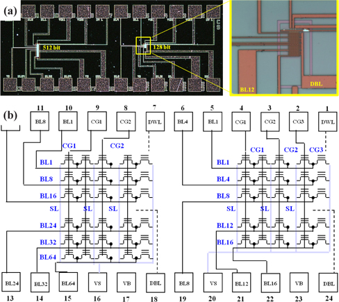
The NOR-type SONOS memory devices used in this study were fabricated using a standard 0.35 μm complementary-metal-oxide-semiconductor (CMOS) technology. In these devices, the channel length and width were 0.5 μm and 0.5 μm, respectively, and the ONO layer thicknesses observed by transmission electron microscopy (TEM) were 3.4 nm/7.3 nm/3.4 nm. The bottom oxide layer was thermally grown at 900℃ in nitrogen diluted with oxygen. To make the ONO stack, the nitride was first deposited using low-pressure chemical-vapor deposition (LPCVD) at a low chamber pressure of 0.5 Torr at 770℃ by reacting dichlorosilane (SiH2Cl2) with ammonia (NH3) = 30 : 330 sccm. The blocking oxide was then grown by thermal oxidation at 950℃ with a gas flow ratio of hydrogen (H2) : oxygen (O2) = 5 : 10 l/min. Sequentially, the n-type impurity was ion implanted to form n+ diffusion layers after the field oxide was etched by self-align source (SAS). Diffusion layers of the n+ type were used for the common source line, and the salicide process was implemented to reduce the resistance of n+ diffusion layers. For all of these SONOS cells, the drains were electrically connected to the bit line (BL) while the gates and the sources were connected to the word line (WL) crossing the BL and the common source line (CSL) for every 128 memory cells
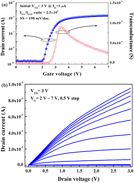
Figure 2(a) shows the drain current-gate voltage (ID-VG) and transconductance curves as a function of drain voltages for the one cell selected within a 128 bit cell array. The transfer characteristics of the selected cell were measured at a drain voltage of 100 mV by sweeping the gate voltage from 0 V to 7 V. The threshold voltage (VTH) was measured to be 3 V. The selected cell showed a high ON/OFF current ratio (ION/IOFF) exceeding 106. The linear transconductance (Gm) was 8.87×10⁻⁶ S at a turn-on voltage. The subthreshold swing (SS) was 198 mV/decade, which may be an acceptable value considering the ideal value of 60 mV/decade. Figure 2(b) shows the drain current-drain voltage (ID-VD) curves as a function of gate voltages applied from 2 V to 7 V with 0.5 V steps. This shows a good n-channel field effect transistor characteristic with typical saturation effects at high drain voltages.
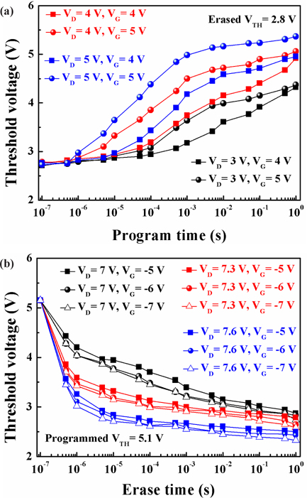
In order to demonstrate the memory effect for the one cell selected within a 128 bit cell array, the (P/E) characteristics using CHEI and HHI methods are shown in Fig. 3. First, the VTH shifts are plotted against the program time at different drain and gate voltages after the VTH of the selected cell was erased at 2.8 V, as shown in Fig. 3(a). As the program voltage and time increased, the VTH increased. A VTH shift of 2 V, which is large enough for program operation, was observed for the 5 V gate and 5 V drain bias conditions at a program time of 5 ms. Second, the erase characteristics are shown in Figure 3(b). The VTH shifts were plotted against the erase time for various drain and gate voltages ranging from 7 V to 7.6 V with 0.3 V steps and from −5 V to −7 V with 1 V steps, after the cell were programmed at a VTH of 5.1 V. The VTH shifts in each programmed state decreased, due to the recombination of the charges injected from the substrate channel to the Si3N4 layer through drain edges. The erasing speed increases with increasing drain or gate voltage. From these results, 7.6 V drain and −6 V gate voltages are determined to be the most suitable erase condition at an erase time of 10 μs.
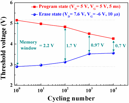
Based on the P/E conditions in Fig. 3, we investigated the endurance characteristics, as shown in Fig. 4.
By increasing the cycling number, the initial memory window of 2.2 V gradually decreased to 1.7 V, however, after 103 P/E cycles, the sensing margin between program and erase states abruptly decreased. This endurance degradation is attributed to the interface-trap generation and the electron trapping in the tunneling oxide [15,16].
In order to verify the endurance degradation, a charge pumping method was employed [17,18]. Here, the charge pumping current (Icp) measurements were carried out as follows: A square pulse was applied to the gate of the selected SONOS cell while the source and substrate were grounded. A current meter (Keithley 4200) was used to measure the Icp from the drain electrode. The gate pulse had a frequency of 1 MHz, a 50% duty cycle, rise/fall times of 10 ns and an amplitude voltage (Va) of 5 V.
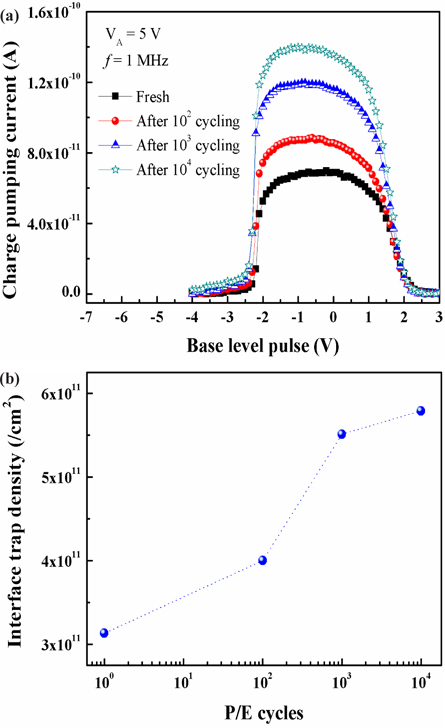
Figure 5(a) shows the charge pumping current (Icp) characteristics for the fresh and different numbers of P/E cycles at the erased state. The Icp curves are plotted by the base level pulse height (Vh) from −4 V to 3 V as a function of the fresh and cycling numbers. By increasing the number of cycles to 102, the maximum Icp gradually increased due to the interface-trap generation. After 103 P/E cycles, the maximum Icp rapidly increased. The interface trap density (Nit) extracted from the Icp curves versus P/E cycle numbers is shown in Fig. 5(b). Compared to the Nit of initial state, the extracted Nit values of 102 cycled state slightly increased from 3.13×1011 cm−2 (initial state) to 4×1011 cm−2. Remarkably, the Nit values from 103 to 104 cycling steeply increased from 5.51×1011 cm−2 to 5.79×1011 cm−2, as compared to the Nit for 102 cycling. The steep increase of the Nit for 103 P/E cycles are consistent with the abrupt endurance degradation for 103 P/E cycles. Consequently, the relationship was determined between the endurance degradation and interface traps using charge pumping methods in actual flash cell array. The endurance properties of 104 cycles may not be enough for memory operation, but could be improved if we used thicker tunnel oxide layer or SiN-layer optimization, as indicated in previous work [19,20].
The relation between the interface traps and the endurance degradation in SONOS devices has been successfully investigated using charge pumping methods, from the one cell selected within a 128 bit cell array. After 103 P/E cycles and above, the memory window abruptly reduced from 2.2 V for initial state to 0.7 V for 104 P/E cycles as well as extracted Nit was steeply increased from 3.13×1011 cm−2 for initial state to 5.79×1012 cm−2 for 104 P/E cycles due to tunnel oxide damage. We conclude P/E-cycling-induced trap generation leads to memory window closure and eventual device degradation is strongly dependent on Nit.